化工进展 ›› 2021, Vol. 40 ›› Issue (S1): 270-280.DOI: 10.16085/j.issn.1000-6613.2021-0216
纳米铜导电墨水在电子印刷线路板制备中的应用进展
王晓芳1( ), 陈嘉苗1, 陆嘉晟1, 罗继业1, 籍少敏1, 霍延平1,2(), 赵经纬2,3(), 方岩雄1()
- 1.广东工业大学轻工化工学院,广东 广州 510006
2.广州天赐高新材料股份有限公司,广东 广州 510006
3.中国科学院上海有机化学研究所有机氟化学重点实验室,上海 200032
-
收稿日期:2020-01-29修回日期:2021-03-08出版日期:2021-10-25发布日期:2021-11-09 -
通讯作者:霍延平,赵经纬,方岩雄 -
作者简介:王晓芳(1994—),女,硕士研究生,研究方向为纳米铜导电墨水制备。E-mail:2322634862@qq.com 。 -
基金资助:国家自然科学基金(21975055);广东省重点领域科技计划(2019A050510042)
Application progress of nano copper conductive ink in PCB
WANG Xiaofang1(), CHEN Jiamiao1, LU Jiasheng1, LUO Jiye1, JI Shaomin1, HUO Yanping1,2(), ZHAO Jingwei2,3(), FANG Yanxiong1()
- 1.School of Light Industry and Chemical Engineering, Guangdong University of Technology, Guangzhou 510006,Guangdong,China
2.Guangzhou Tianci High-tech Materials Company Limited, Guangzhou 510006, Guangdong, China
3.Shanghai Institute of Organic Chemistry, Chinese Academy of Sciences, Key Laboratory of Organofluorine Chemistry, Shanghai 200032, China
-
Received:2020-01-29Revised:2021-03-08Online:2021-10-25Published:2021-11-09 -
Contact:HUO Yanping,ZHAO Jingwei,FANG Yanxiong
摘要:
近年来,随着电子行业的发展,人们更多开始关注纳米材料在电子印刷电路板(printed circuit board,PCB)中的应用,新型、高效、经济、环保的技术方法逐渐替代传统制造工艺。本文综述了不同种纳米材料导电墨水的制备方法和新型印制电路板制备技术的发展,通过对比不同反应物、添加剂以及不同方法对最终生成的纳米铜导电墨水性能的影响,针对性介绍了适应于不同要求的纳米材料制备工艺技术。此外,介绍了不同的烧结工艺和打印工艺对最终生成PCB线路的影响。相对于传统的覆铜板刻蚀电路技术污染大、材料浪费、工艺复杂等缺点,新工艺结合纳米材料性能,利用高精度设备,着重向低成本、少污染、时间短、能耗低的方向进行一系列研究,文章还讨论了未来PCB行业在5G的应用发展方向和可能遇到的机遇和挑战。
中图分类号:
引用本文
王晓芳, 陈嘉苗, 陆嘉晟, 罗继业, 籍少敏, 霍延平, 赵经纬, 方岩雄. 纳米铜导电墨水在电子印刷线路板制备中的应用进展[J]. 化工进展, 2021, 40(S1): 270-280.
WANG Xiaofang, CHEN Jiamiao, LU Jiasheng, LUO Jiye, JI Shaomin, HUO Yanping, ZHAO Jingwei, FANG Yanxiong. Application progress of nano copper conductive ink in PCB[J]. Chemical Industry and Engineering Progress, 2021, 40(S1): 270-280.
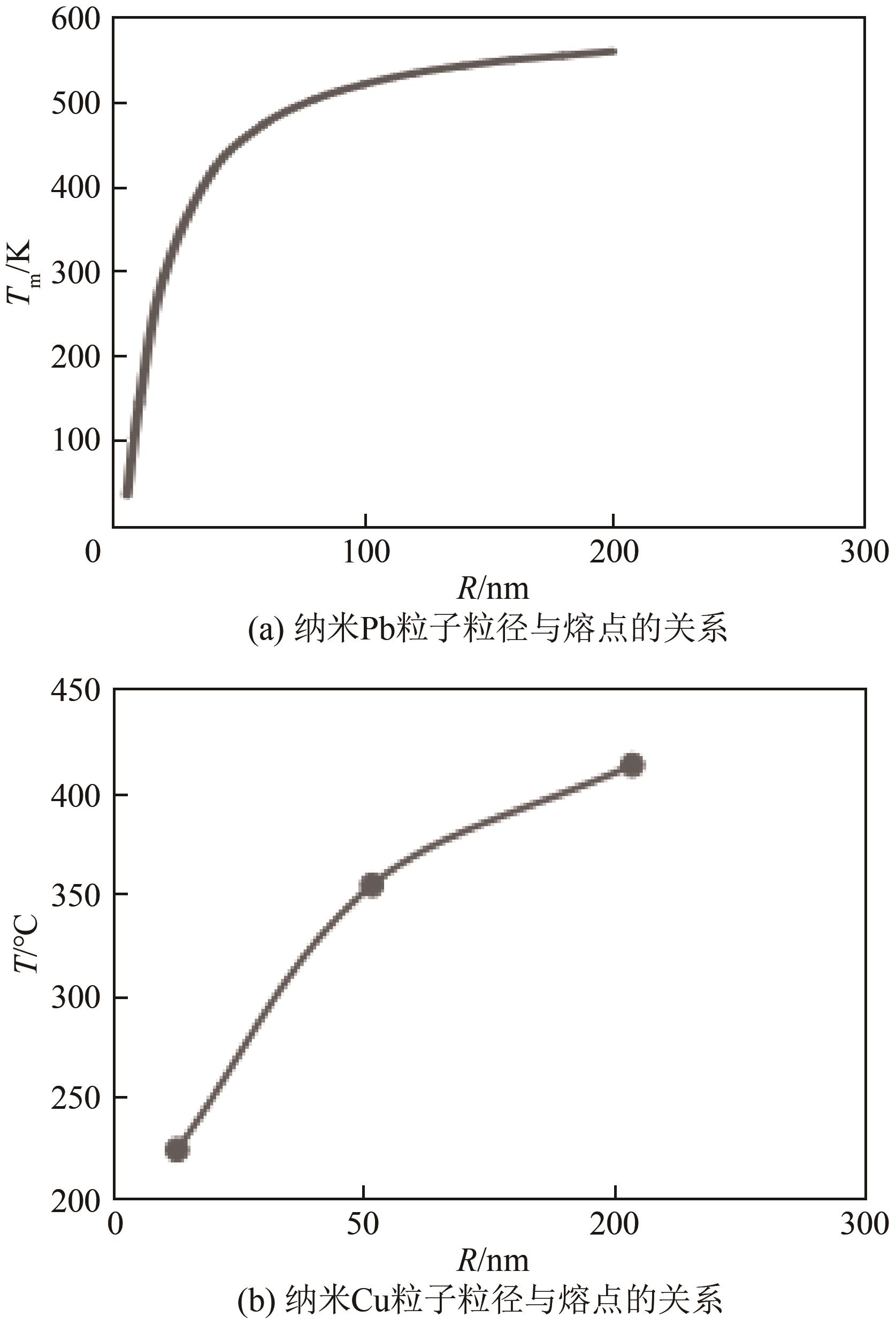
图1 不同金属粒径与熔点的关系[9-10]
| 金属 | 电阻率/μΩ·cm-1 | 熔点/℃ | 价格/CNY·g-1 |
|---|---|---|---|
| 金 | 2.40 | 1064 | 250~550 |
| 银 | 1.65 | 961 | 4~6 |
| 铜 | 1.75 | 1084 | 0.027~0.052 |
表1 3种金属性能对照表
| 金属 | 电阻率/μΩ·cm-1 | 熔点/℃ | 价格/CNY·g-1 |
|---|---|---|---|
| 金 | 2.40 | 1064 | 250~550 |
| 银 | 1.65 | 961 | 4~6 |
| 铜 | 1.75 | 1084 | 0.027~0.052 |
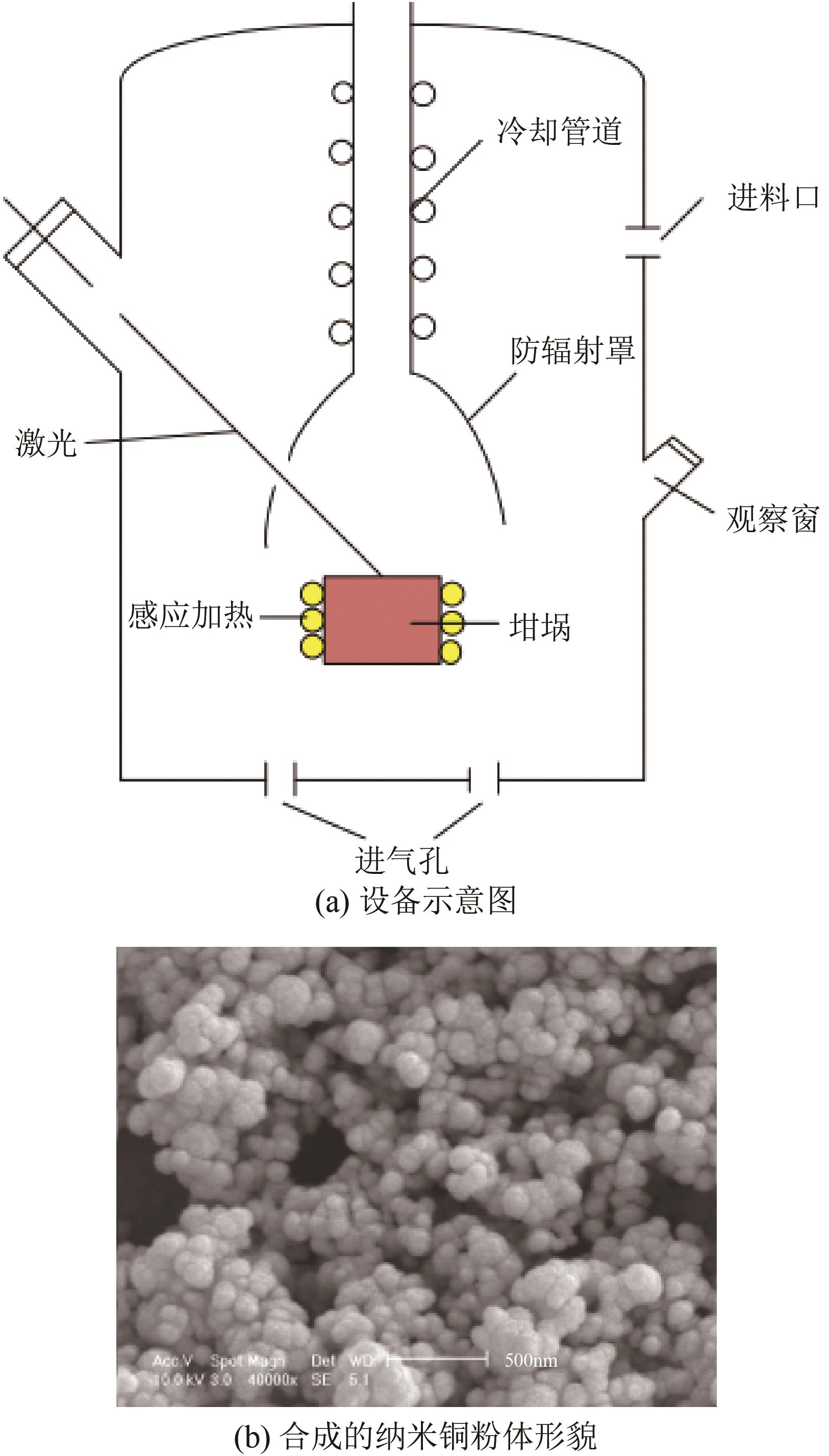
图2 激光加热蒸发设备及其制备的超细纳米铜微观形貌[20]
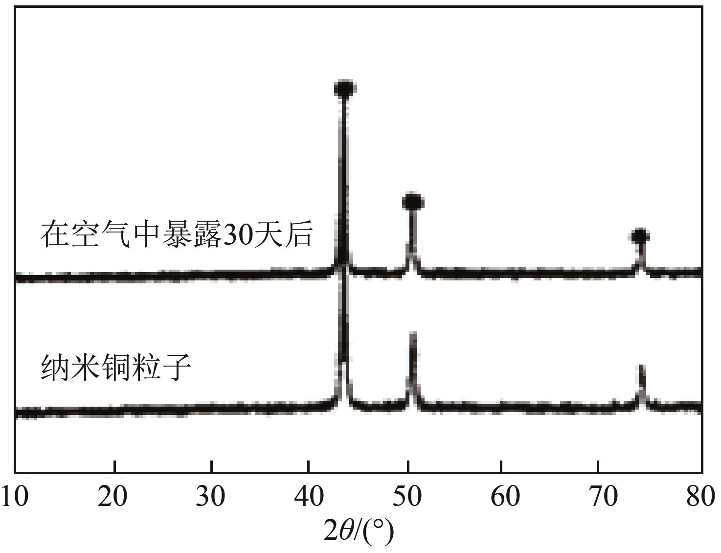
图3 合成的纳米铜及其空气中暴露30天后XRD对比图

图4 不同条件和添加剂浓度对纳米铜粒径影响[35]

图5 不同印刷方式的原理
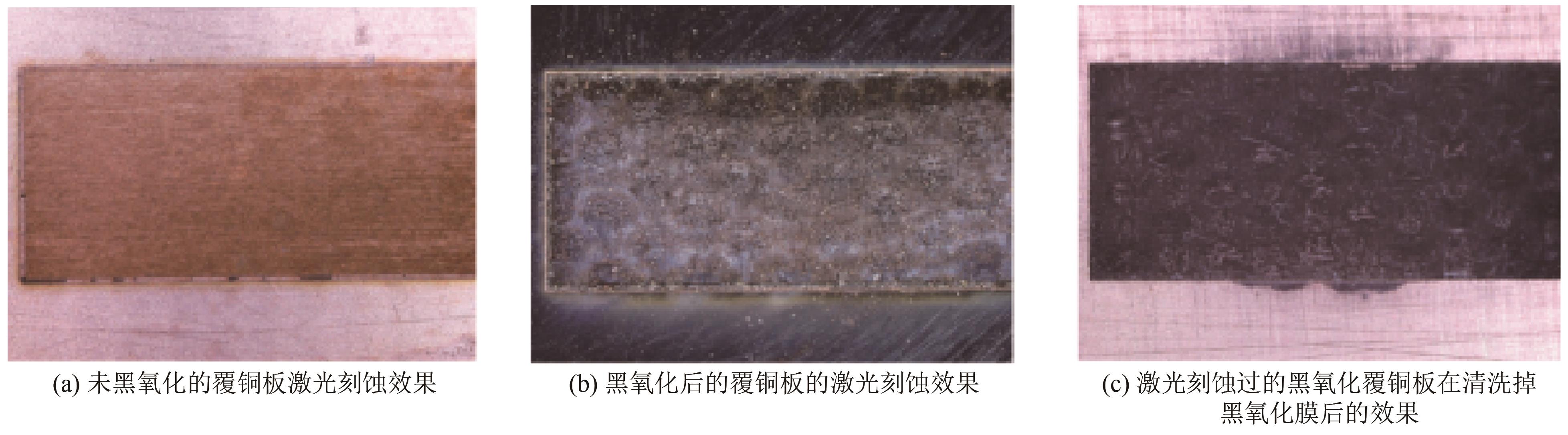
图6 黑氧化工艺对激光刻蚀的影响[46]

图7 被氧化前后表面铜箔SEM图[46]
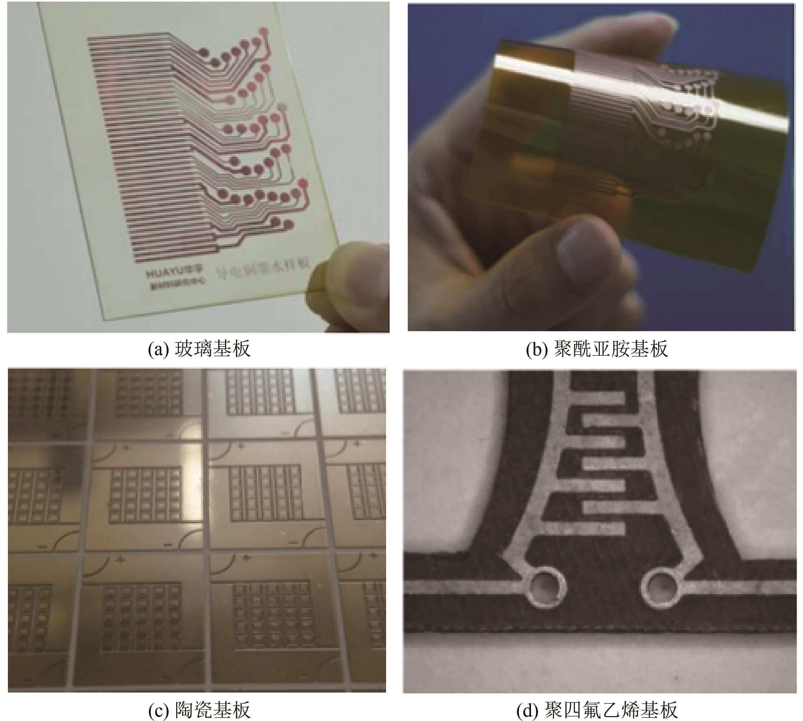
图8 不同基板的印制线路效果[10,43]
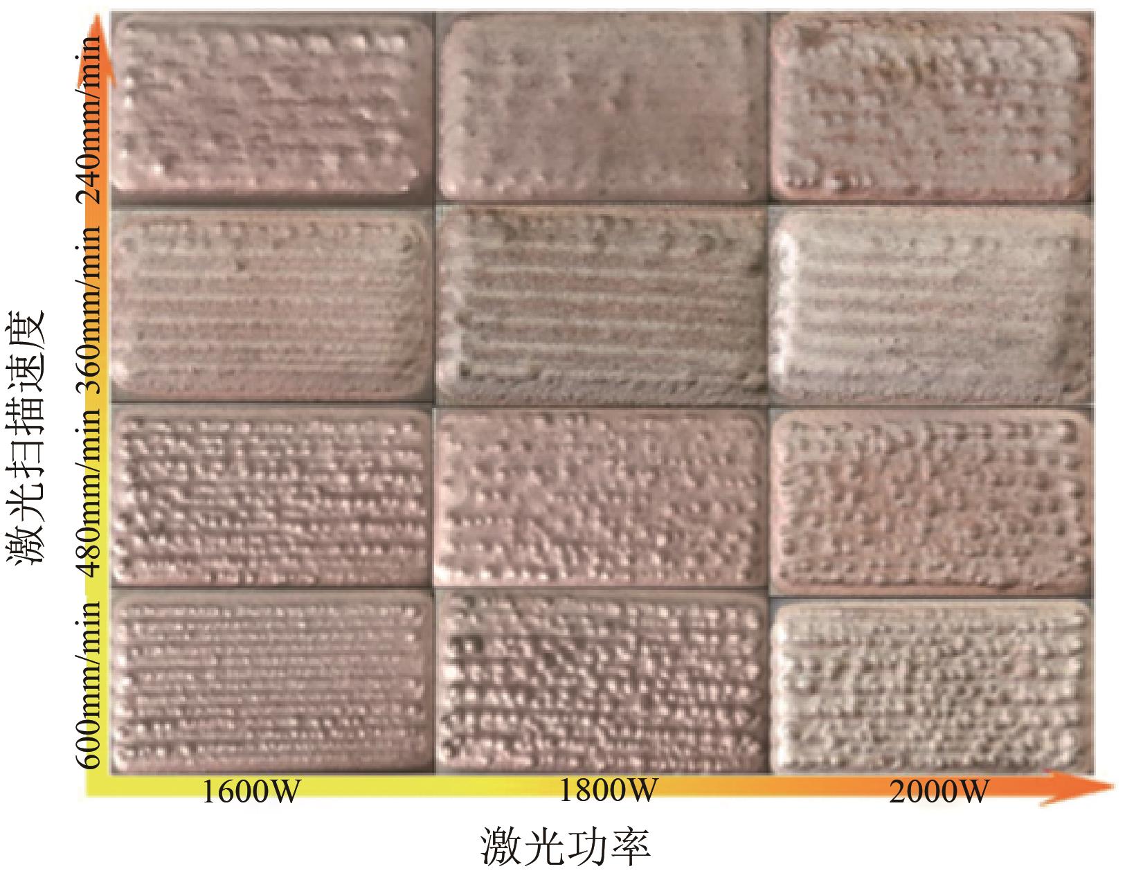
图9 钨铜复合材料在不同激光功率和扫描速度下的宏观形貌[49]
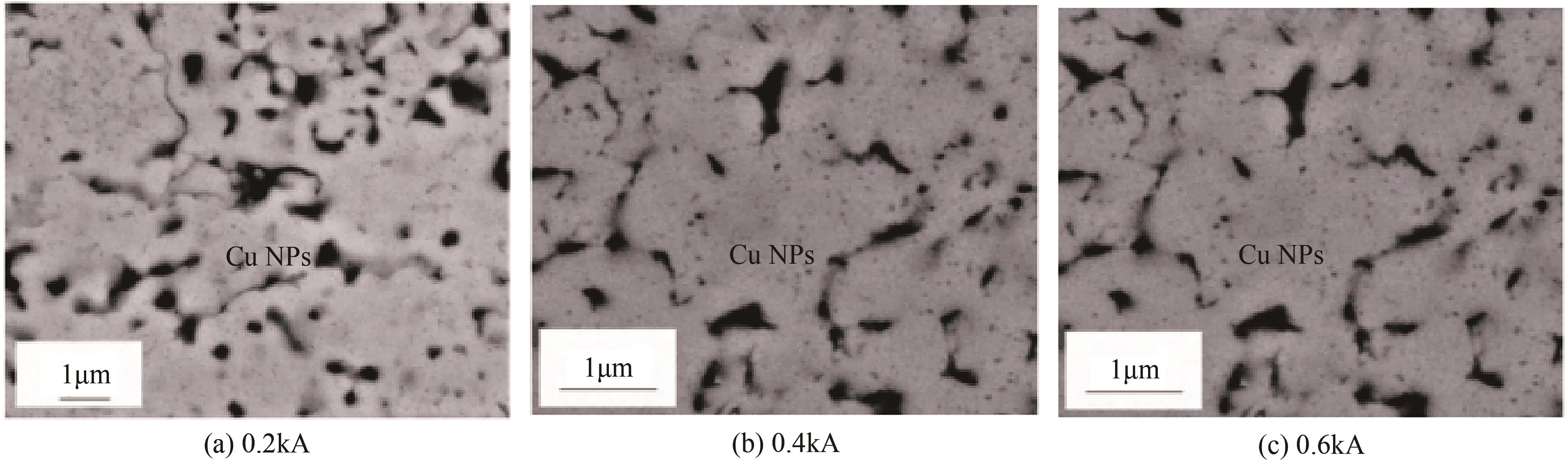
图10 不同电流烧结得到的SEM图[50]
| 1 | 张念椿, 刘彬云, 王恒义. 全印制电路技术导电油墨的新型材料纳米铜制备[J]. 材料研究与应用, 2010, 4(4): 428-432. |
| ZHANG Nianchun, LIU Binyun, WANG Hengyi. Full printed electronics: preparation new materials nano-copper in conductive ink[J]. Materials Research and Application, 2010, 4(4): 428-432. | |
| 2 | KIM H S, KANG J S, PARK J S, et al. Inkjet printed electronics for multifunctional composite structure[J]. Composites Science and Technology, 2009, 69(7/8): 1256-1264. |
| 3 | WONG W S, DANIEL J H, CHABINYC M L, et al. Organic electronics: materials, manufacturing and applications[M]. Weinheim: Wiley-VCH Verlag GmbH & Co. KGaA, 2006: 271-293. |
| 4 | KWON Y T, LEE Y I, LEE K J, et al. A novel method for fine patterning by piezoelectrically induced pressure adjustment of inkjet printing[J]. Journal of Electronic Materials, 2015, 44(8): 2608-2614. |
| 5 | 庄严. 印刷电子学的发展[J]. 电子元件与材料, 2010, 29(9): 1-5. |
| ZHUANG Yan. Development of printed electronics[J]. Electronic Components and Materials, 2010, 29(9): 1-5. | |
| 6 | 李瑞. 网印导电油墨的种类及其应用[J]. 丝网印刷, 2010(6): 30-32. |
| LI Rui. Types and applications of screen printing conductive ink[J]. Screen Printing, 2010(6): 30-32. | |
| 7 | LEUNG S Y Y, LAM D C C. Geometric and compaction dependence of printed polymer-based RFID tag antenna performance[C]//International Conference on Electronic Materials and Packaging, 2007. |
| 8 | 林金堵. 喷墨打印技术在PCB中的应用前景[J]. 印制电路信息, 2008, 16(4): 8-13. |
| LIN Jindu. The application prospect of inkjet printing technology in PCB[J]. Printed Circuit Information, 2008, 16(4): 8-13. | |
| 9 | 瞿金蓉, 胡明安, 陈敬中, 等. 纳米粒子的熔点与粒径的关系[J]. 地球科学, 2005, 30(2): 195-198. |
| QU Jinrong, HU Mingan, CHEN Jingzhong, et al. Nanoparticle size and melting point relationship[J]. Earth Science, 2005, 30(2): 195-198. | |
| 10 | 李健. 纳米铜导电油墨工艺及应用研究[D]. 武汉: 华中科技大学, 2012. |
| LI Jian. Processing and application research of nano copper conductive ink[D]. Wuhan: Huazhong University of Science and Technology, 2012. | |
| 11 | 王晓霞, 叶红齐, 苏周, 等. 超细铜粉的制备与应用[J]. 材料导报, 2004, 18(S2): 140-142. |
| WANG Xiaoxia, YE Hongqi, SU Zhou, et al. The preparation of ultrafine copper powder and its application[J]. Materials Review, 2004, 18(S2): 140-142. | |
| 12 | 胡良. 超细纳米金的制备和银纳米线的改性及其二氧化碳电催化还原性能的研究[D]. 杭州: 浙江大学, 2019. |
| HU Liang. Preparation of ultrasmall Au NPs and modification of Ag NWs and their CO2 electroreduction performances[D]. Hangzhou: Zhejiang University, 2019. | |
| 13 | LEE K J, JUN B H, LEE Y I, et al. Metal nano particle and method for manufacturing them and conductive ink: US20060254387[P]. 2006-11-16. |
| 14 | 林荣会, 方亮, 郗英欣, 等. 化学还原法制备纳米铜[J]. 化学学报, 2004, 62(23): 2365-2368. |
| LIN Ronghui, FANG Liang, XI, yingxin, et al. Preparation of nanoparticle copper by chemical reduction[J]. Acta Chimica Sinica, 2004, 62(23): 2365-2368. | |
| 15 | SEONG M R, KWON J, LEE G Y, et al. Optimization of surface coating condition using vapor form of alkanethiol on Cu nano powders for the application of oxidation prevention[J]. Applied Surface Science, 2010, 256(8): 2332-2336. |
| 16 | 邓吨英, 肖斐. 纳米铜油墨和铜导电薄膜的制备方法: CN102924996A[P]. 2013-02-13. |
| DENG Dunying, XIAO Fei. Preparation method of nano copper ink and copper conductive film: CN102924996A[P]. 2013-02-13. | |
| 17 | 陈嘉君, 王涵, 宋西平. 物理气相沉积法制备镁纳米线的工艺及机理[J]. 材料热处理学报, 2016, 37(S1): 1-4. |
| CHEN Jiajun, WANG Han, SONG Xiping. Process and mechanism of magnesium nanowires prepared by physical vapor deposition[J]. Transactions of Materials and Heat Treatment, 2016, 37(S1): 1-4. | |
| 18 | 杨小健, 何为, 王守绪, 等. 用喷墨打印法直接形成铜导电线路图形[J]. 印制电路信息, 2009, 17(11): 28-31, 35. |
| YANG Xiaojian, HE Wei, WANG Shouxu, et al. Copper conductive patterns direct writing by ink-jet printing[J]. Printed Circuit Information, 2009, 17(11): 28-31, 35. | |
| 19 | DORDA Feliks. A method of obtaining ultra-dispersive copper powder by supplying copper nitrate solution into nitrogen plasma[J]. Russian Physics Journal,1996,7:271. |
| 20 | 谢长生, 胡军辉, 陶曾毅, 等. 加热蒸发制备超微粉的方法和设备:CN240687A[P]. 2000-01-12. |
| XIE Changsheng, HU Junhui, TAO Zengyi, et al. Method and equipment for preparing ultrafine powder by heating evaporation: CN240687A[P]. 2000-01-12. | |
| 21 | 于庆杰, 王祥彬. 超声波在超细粉体分散中的应用[J]. 聚酯工业, 2004, 17(3): 32-33. |
| YU Qingjie, WANG Xiangbin. Application of ultrasonic in the dispersion of ultrafine powder[J]. Polyester Industry, 2004, 17(3): 32-33. | |
| 22 | 庞真丽, 蒋武锋, 郝素菊, 等. 碳纳米管在水中分散性能[J]. 河北理工大学学报, 2007, 29(1): 97-101. |
| PANG Zhenli, JIANG Wufeng, HAO Suju, et al. The study of dispersion property of carbon nanotubes in water[J]. Journal of Hebei Institute of Technology, 2007, 29(1): 97-101. | |
| 23 | 刘维平. 采用改进型振动球磨机制备超细铜粉的研究[J]. 江西科学, 2000, 18(1): 24-27. |
| LIU Weiping. Study on the preparation of ultra-fine copper powder by improved vibration mill[J]. Jiangxi Science, 2000, 18(1): 24-27. | |
| 24 | 安少华, 张振忠, 段志伟, 等. 不同分散剂对纳米铜粉在乙醇中的分散性能研究[J]. 铸造技术, 2007, 28(11): 1498-1501. |
| AN Shaohua, ZHANG Zhenzhong, DUAN Zhiwei, et al. Study on the effect of different surfactants on dispersing properties of nanometer-scale copper powders in the alcohol solvent[J]. Foundry Technology, 2007, 28(11): 1498-1501. | |
| 25 | 李金平, 吴疆, 梁德青, 等. 纳米粒子悬浮液中分散剂选择的实验研究[J]. 兰州理工大学学报, 2006, 32(3): 63-66. |
| LI Jinping, WU Jiang, LIANG Deqing, et al. Experimental investigation of dispersant selection for preparing nano-particle suspension fluids[J]. Journal of Lanzhou University of Technology, 2006, 32(3): 63-66. | |
| 26 | 李红, 单丹, 高德玉, 等. 金属纳米铜制备技术[J]. 化学工程师, 2007, 21(12): 23-25. |
| LI Hong, SHAN Dan, GAO Deyu, et al. Preparation technology of metal nanocopper[J]. Chemical Engineer, 2007, 21(12): 23-25. | |
| 27 | 陈祖耀, 陈波, 钱逸泰, 等. γ射线辐照-水热结晶联合法制备金属超微粒子[J]. 金属学报, 1992, 28(4): 73-76. |
| CHEN Zuyao, CHEN Bo, QIAN Yitai, et al. Preparation of ultrafine metallic particles by γ-ray radiation hydrothermal crystallization combined method[J]. Acta Metallrugica Sinica, 1992, 28(4): 73-76. | |
| 28 | 林硕, 吴年强, 李志章. 铜系复合涂料导电稳定性的研究[J]. 功能材料, 1999, 30(3): 288-289. |
| LIN Shuo, WU Nianqiang, LI Zhizhang. Study on the conductivity stability of copper-filled composite paint[J]. Journal of Functional Materials, 1999, 30(3): 288-289. | |
| 29 | LUECHINGER N A, ATHANASSIOU E K, STARK W J. Graphene-stabilized copper nanoparticles as an air-stable substitute for silver and gold in low-cost ink-jet printable electronics[J]. Nanotechnology, 2008, 19(44): 445201. |
| 30 | 黄涛. 基于直写的纳米银导电浆料及导电墨水的研制[D]. 武汉: 华中科技大学, 2009. |
| HUANG Tao. Study on the nano-silver paste and nano-silver ink for direct writing[D]. Wuhan: Huazhong University of Science and Technology, 2009. | |
| 31 | 刘欣, 彭莉岚, 冯鹏元, 等. 多元醇法形貌可控制备氧化亚铜微纳米颗粒[J]. 应用化学, 2018, 35(4): 469-476. |
| LIU Xin, PENG Lilan, FENG Pengyuan, et al. Morphology control of cuprous oxide micro-and nanoparticles by polyol method[J]. Chinese Journal of Applied Chemistry, 2018, 35(4): 469-476. | |
| 32 | 施静敏. 3D打印用纳米铜粉的调控制备与激光烧结模拟[D]. 北京: 有色金属研究总院, 2019. |
| SHI Jingmin. Regulated preparation and laser sintering simulation of nano copper powder for 3D printing[D]. Beijing: Nonferrous Metal Research Institute, 2019. | |
| 33 | XIONG J, WANG Y, XUE Q J, et al. Synthesis of highly stable dispersions of nanosized copper particles using l-ascorbic acid[J]. Green Chemistry, 2011, 13(4): 900. |
| 34 | KOROLEVA M Y, KOVALENKO D A, SHKINEV V M, et al. Synthesis of copper nanoparticles stabilized by polyoxyethylenesorbitan monooleate[J]. Russian Journal of Inorganic Chemistry, 2011, 56(1): 6-10. |
| 35 | 聂昆深. 纳米铜导电墨水的研制[D]. 广州: 广东工业大学, 2013. |
| NIE Kunshen. Development of nano-copper conductive ink[D]. Guangzhou: Guangdong University of Technology, 2013. | |
| 36 | 李新芳, 朱冬生, 王先菊, 等. 纳米Cu分散稳定性能影响因素及作用机理研究[J]. 化学工程, 2007, 35(12): 46-50. |
| LI Xinfang, ZHU Dongsheng, WANG Xianju, et al. Effect factor and function mechanism on dispersion and stability of Cu nanoparticles[J]. Chemical Engineering, 2007, 35(12): 46-50. | |
| 37 | TANG X F, YANG Z G, WANG W J. A simple way of preparing high-concentration and high-purity nano copper colloid for conductive ink in inkjet printing technology[J]. Colloids and Surfaces A: Physicochemical and Engineering Aspects, 2010, 360(1/2/3): 99-104. |
| 38 | 许伟, 姚日晖, 宁洪龙. 喷墨打印技术制备柔性导电聚合物薄膜图案[J]. 实验技术与管理, 2019, 36(8): 52-56. |
| XU Wei, YAO Rihui, NING Honglong. Preparation on pattern of flexible conductive polymer film by inkjet printing technology[J]. Experimental Technology and Management, 2019, 36(8): 52-56. | |
| 39 | ROZMAN R, KMETEC B, PODOBNIK B, et al. Optimisation of direct laser structuring of printed circuit boards[J]. Applied Surface Science, 2008, 254(17): 5524-5529. |
| 40 | 姚丽丽. PCB线路选择性激光镀蚀工艺的实验研究[D]. 广州: 广东工业大学, 2018. |
| YAO Lili. Experimental research on selective laser etching process of PCB lines[D]. Guangzhou: Guangdong University of Technology, 2018. | |
| 41 | AKAMATSU K, IKEDA S, NAWAFUNE H. Site-selective direct silver metallization on surface-modified polyimide layers[J]. Langmuir, 2003, 19(24): 10366-10371. |
| 42 | WU Z P, WU D Z, YANG W T, et al. Preparation of highly reflective and conductive metallized polyimide films through surface modification: processing, morphology and properties[J]. J. Mater. Chem., 2006, 16(3): 310-316. |
| 43 | 徐璞. 基于激光直写电路技术的PCB板快速制造系统[J]. 新技术新工艺, 2019(3): 58-62. |
| XU Pu. PCB board rapid manufacturing system based on laser direct writing circuit technology[J]. New Technology & New Process, 2019(3): 58-62. | |
| 44 | 李林, 李正佳, 何艳艳. 全固态紫外激光器研究进展[J]. 激光杂志, 2005, 26(6): 1-3. |
| LI Lin, LI Zhengjia, HE Yanyan. Progress of search on all solid-state ultraviolet laser[J]. Laser Journal, 2005, 26(6): 1-3. | |
| 45 | 耿广刚. 激光热处理用吸光涂层材料的设计与优化[D]. 杭州: 浙江工业大学, 2011. |
| GENG Guanggang. Design and optimization of light-absorbing coating materials for laser heat treatment[D]. Hangzhou: Zhejiang University of Technology, 2011. | |
| 46 | 姚丽丽, 李瑜煜. 便于激光刻蚀的PCB基板铜箔表面黑氧化工艺[J]. 电镀与涂饰, 2018, 37(9): 386-390. |
| YAO Lili, LI Yuyu. Black oxidation of copper foil on PCB basilar plate for laser etching[J]. Electroplating & Finishing, 2018, 37(9): 386-390. | |
| 47 | 刘清源, 王英志, 胡俊. PCB激光制版曝光误差分析及校正[J]. 电子技术与软件工程, 2018(5): 77. |
| LIU Qingyuan, WANG Yingzhi, HU Jun. Analysis and correction of PCB laser exposure error[J]. Electronic Technology and Software Engineering, 2018(5): 77. | |
| 48 | 左兰兰, 陈艳, 王远鑫. 微波场中铜粉烧结行为的初步研究[J]. 安徽工业大学学报(自然科学版), 2008, 25(2): 117-119, 127. |
| ZUO Lanlan, CHEN Yan, WANG Yuanxin. Research on the sintering of copper powder under microwave irradiation[J]. Journal of Anhui University of Technology (Natural Science Edition), 2008, 25(2): 117-119, 127. | |
| 49 | LIU Z H, ZHOU W C, LU Y Z, et al. Laser 3D printing of W-Cu composite[J]. Materials Letters, 2018, 225: 85-88. |
| 50 | 黄圆, 田艳红, 江智, 等. 脉冲电流快速烧结纳米铜焊膏连接铜镍基板研究[J]. 机械工程学报, 2017, 53(4): 34-42. |
| HUANG Yuan, TIAN Yanhong, JIANG Zhi, et al. Rapidly sintering of nano copper paste and interconnection of copper and nickel substrate by pulse current[J]. Journal of Mechanical Engineering, 2017, 53(4): 34-42. |
| [1] | 邵志国, 任雯, 许世佩, 聂凡, 许毓, 刘龙杰, 谢水祥, 李兴春, 王庆吉, 谢加才. 终温对油基钻屑热解产物分布和特性影响[J]. 化工进展, 2023, 42(9): 4929-4938. |
| [2] | 杨莹, 侯豪杰, 黄瑞, 崔煜, 王兵, 刘健, 鲍卫仁, 常丽萍, 王建成, 韩丽娜. 利用煤焦油中酚类物质Stöber法制备碳纳米球用于CO2吸附[J]. 化工进展, 2023, 42(9): 5011-5018. |
| [3] | 尹新宇, 皮丕辉, 文秀芳, 钱宇. 特殊浸润性材料在防治油气管道中水合物成核与聚集的应用[J]. 化工进展, 2023, 42(8): 4076-4092. |
| [4] | 高聪, 陈城虎, 陈修来, 刘立明. 代谢工程改造微生物合成生物基单体的进展与挑战[J]. 化工进展, 2023, 42(8): 4123-4135. |
| [5] | 姜晶, 陈霄宇, 张瑞妍, 盛光遥. 载锰生物炭制备及其在环境修复中应用研究进展[J]. 化工进展, 2023, 42(8): 4385-4397. |
| [6] | 吴亚, 赵丹, 方荣苗, 李婧瑶, 常娜娜, 杜春保, 王文珍, 史俊. 用于复杂原油乳液的高效破乳剂开发及应用研究进展[J]. 化工进展, 2023, 42(8): 4398-4413. |
| [7] | 徐沛瑶, 陈标奇, KANKALA Ranjith Kumar, 王士斌, 陈爱政. 纳米材料用于铁死亡联合治疗的研究进展[J]. 化工进展, 2023, 42(7): 3684-3694. |
| [8] | 许春树, 姚庆达, 梁永贤, 周华龙. 氧化石墨烯/碳纳米管对几种典型高分子材料的性能影响[J]. 化工进展, 2023, 42(6): 3012-3028. |
| [9] | 张晨宇, 王宁, 徐洪涛, 罗祝清. 纳米颗粒强化传热的多级潜热储热器性能评价[J]. 化工进展, 2023, 42(5): 2332-2342. |
| [10] | 陈少华, 王义华, 胡强飞, 胡坤, 陈立爱, 李洁. 电化学修饰电极在检测Cr(Ⅵ)中的研究进展[J]. 化工进展, 2023, 42(5): 2429-2438. |
| [11] | 刘宇龙, 姚俊虎, 舒闯闯, 佘跃惠. 磁性Fe3O4纳米颗粒的生物合成及其在提高采收率中的应用[J]. 化工进展, 2023, 42(5): 2464-2474. |
| [12] | 殷铭, 郭晋, 庞纪峰, 吴鹏飞, 郑明远. 铜催化剂在涉氢反应中的失活机制和稳定策略[J]. 化工进展, 2023, 42(4): 1860-1868. |
| [13] | 葛伟童, 廖亚龙, 李明原, 嵇广雄, 郗家俊. Pd-Fe/MWCNTs双金属催化剂制备及其脱氯动力学[J]. 化工进展, 2023, 42(4): 1885-1894. |
| [14] | 万茂华, 张小红, 安兴业, 龙垠荧, 刘利琴, 管敏, 程正柏, 曹海兵, 刘洪斌. MXene在生物质基储能纳米材料领域中的应用研究进展[J]. 化工进展, 2023, 42(4): 1944-1960. |
| [15] | 司银芳, 胡语婕, 张凡, 董浩, 佘跃惠. 生物合成氧化锌纳米颗粒材料及其抗菌应用[J]. 化工进展, 2023, 42(4): 2013-2023. |
| 阅读次数 | ||||||
|
全文 |
|
|||||
|
摘要 |
|
|||||